

Building a New Era in Smart Manufacturing Safety: Breakthroughs in SMT Inspection Technology
December 19, 2024The productronica Shanghai, a crucial platform for showcasing and exchanging ideas in the electronic intelligent manufacturing industry, will grandly resume from March 26 to 28, 2025, in Halls E1-E5 & W1-W3 of the Shanghai New International Expo Centre (SNIEC). This exhibition will be extensive, covering nearly 100,000 square meters. It is expected to attract nearly 1,000 quality enterprises from the electronics manufacturing industry. They will showcase products and technologies spanning the entire electronic manufacturing supply chain, including electronic and chemical materials, dispensing and gluing technologies, electronic assembly automation, testing, measurement, and quality assurance, electronic manufacturing services, surface mount technology (SMT), harness processing and connector manufacturing, component and part manufacturing, motion control and drive technology, industrial sensors, robotics, and intelligent warehousing, among others.
The rapid growth of the global electronics industry, coupled with increasing product sophistication, has led to the widespread adoption of Surface Mount Technology (SMT) processing. A unanimous choice for many enterprises, SMT delivers exceptional efficiency, precision, and cost-effectiveness. This shift in technology has fueled substantial growth in the electronics inspection sector. The performance and reliability of modern electronic products are fundamentally dependent on the precision, density, and sophistication of their printed circuit boards (PCBs). Minor soldering defects, including insufficient solder, bridging, or internal voids, can lead to product failure. A survey conducted by QY Research projects that the global SMT inspection equipment market will reach USD 1.2 billion by 2029, with a compound annual growth rate (CAGR) of 4.7% over the coming years. SMT inspection technology is continually evolving to ensure that each solder joint meets high standards, addressing the rigorous demands of miniaturized and high-density electronic components and assembly boards with high speeds in signal processing.
AOI, AI, and 3D technologies create an impeccable inspection framework to tackle the challenge of circuit board miniaturization
As circuit board sizes decrease, the challenges associated with manual inspection have increased. Consequently, Automated Optical Inspection (AOI) has emerged as a vital technology for assessing the quality of SMT assembly. As a crucial tool for defect control, AOI can accurately detect and rectify errors during the early stages of the assembly process, thereby enhancing overall process management. Early defect detection through AOI not only prevents defective products from entering subsequent assembly stages but also reduces maintenance costs and prevents circuit board waste due to irreparable damage, ultimately enhancing manufacturing efficiency and yield rates.
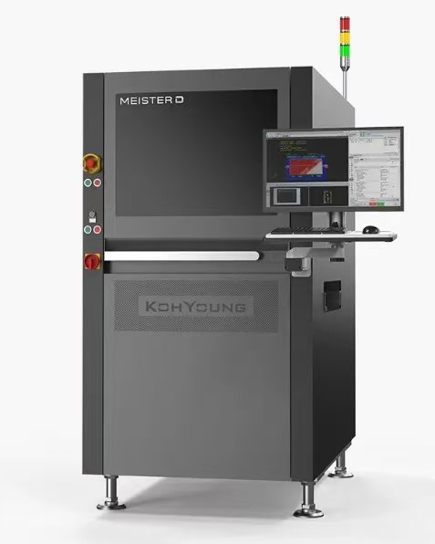
Koh Young Technology's Meister D and Meister D+ are 3D AOI solutions tailored for inspecting high-density substrates and specular material components. Utilizing these technologies guarantees a zero-defect production process. Meister D offers outstanding 3D inspection services for dies and small components, including those as tiny as 0201 (metric system) components. The system also accommodates components with pitches as narrow as 50 µm, guaranteeing precise measurements regardless of the Die or LED characteristics. Meister D+ further enhances the inspection capabilities of specular material components by integrating Moiré measurement and inspection technology with Koh Young Technology's innovative optical technology. This combination enables comprehensive 3D height and tilt inspection of highly reflective Die components.
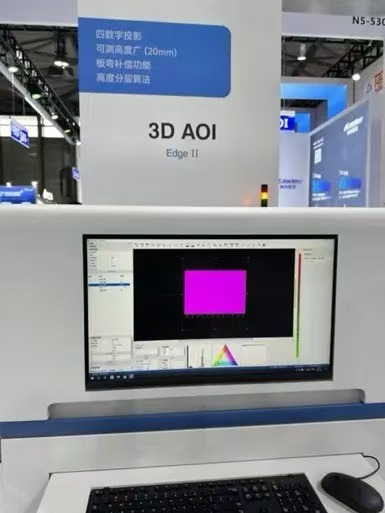
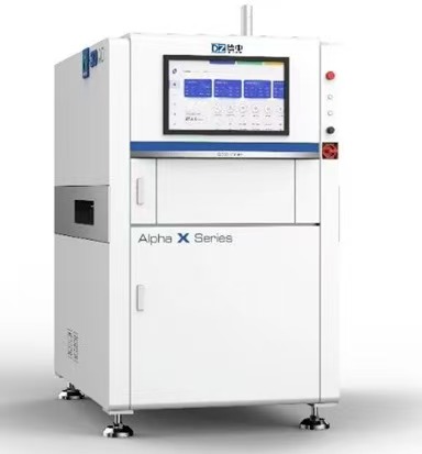
The widespread use of miniature components such as 01005 and 0201 has rendered traditional 2D AOI methods insufficient. 2D AOI, which relies exclusively on two-dimensional image data, falls short of delivering the comprehensive, multi-dimensional inspection coverage necessary to meet the high-quality service demands of a rapidly evolving market. In response to this demand, Shanghai-based Jutze Technology has launched its next-generation fully automated 3D optical inspection equipment, the 3D AOI II. This system, designed for in-line PCB appearance inspections, is a seamless combination of 2D and 3D machine technologies. This product employs variable-frequency digital grating projection technology to capture 3D images and accurately detect components at different heights. It effectively overcomes traditional 2D inspection limitations, particularly in identifying tilted or warped components. Additionally, the all-new second-generation 3D AOI equipment incorporates a new motion module consisting of a linear motor and a grating ruler, significantly enhancing product inspection efficiency. The previous 3D four-digit projection system can be integrated with an imaging system that may include a Z-axis and angled cameras. This configuration offers improved inspection coverage, enabling comprehensive inspection and multi-angle illumination.
A next-generation 3D AOI system, independently developed by VCTA, nears launch. The third-generation dual-drive gantry platform delivers enhanced repeatability and positioning precision, with the flexibility to incorporate either servo or direct drive systems according to specific customer accuracy requirements. It is the first solution of its kind to utilize AI technology, facilitating automated database matching for accelerated programming and enhancing programming efficiency by more than 80%. The AI-powered Optical Character Recognition (AI-OCR) algorithm accurately processes and recognizes inscriptions on parts. It effectively resolves issues such as character blurriness, stroke connection, stroke breakage, and character contamination, while significantly reducing the misjudgment rate associated with variations in character composition. The fully digital structured light 3D reconstruction system maintains consistent accuracy in 3D modeling modules throughout its operational lifespan of up to 10 years. The high-speed industrial camera that captures nearly 200 frames per second provides pixel options of 12 MP and 25 MP, along with a range of resolution options from 5 to 15 μm, to meet diverse application requirements. The software provides extensive support, including offline programming, in-line debugging without downtime, centralized control, and multi-point alignment capabilities, among other features. It integrates with SPC (Statistical Process Control) systems, providing detailed data analytics for optimizing electronic manufacturing processes.

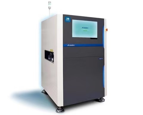
Aleader's 3D AOI technology is distinguished by its three-dimensional imaging capabilities. Aleader's 3D AOI employs a cutting-edge proprietary optical system and advanced image processing technology, delivering exceptional precision and an extensive measurement range. It captures high-quality 2D images while simultaneously conducting shadow-free 3D measurements, thereby improving the comprehensiveness and accuracy of inspection. This unique three-dimensional imaging technology addresses the inspection requirements for the smallest components and solder joints. As a result, Aleader's 3D AOI equipment is capable of handling complex inspections and catering to the special needs of various industries. This technology employs several internationally advanced patented algorithms that are crucial for 3D AOI, enhancing both accuracy and efficiency. These algorithms have been meticulously optimized and tested to accurately detect a range of surface defects on objects, such as minor warps, depressions, and flatness irregularities. They can also automatically modify the inspection parameters to meet the inspection requirements for different objects, ensuring both the accuracy and reliability of the results.
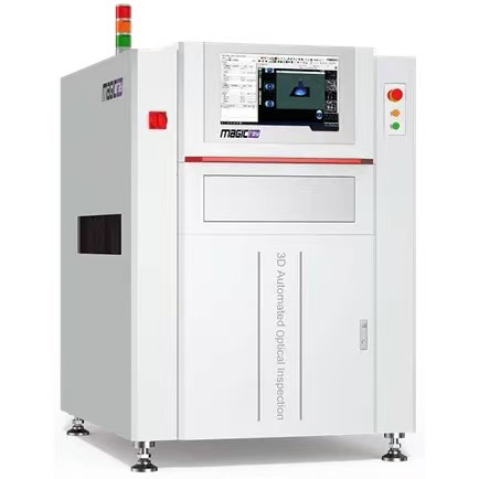
Magic-ray's latest blockbuster product, the double-sided 3D AOI-VS7300, features high precision and speed. It employs a synchronous movement and asynchronous interlocking camera mechanism that effectively avoids light source interference, enabling fast and accurate double-sided inspection and doubling efficiency. The multi-axis high-speed control card features advanced motion control technology, achieving a 3D inspection speed of 450 ms/FOV (single-sided). It also employs sophisticated 3D visual inspection technology that precisely processes point cloud data at the pixel level. The adaptive stripe system effectively captures ultra-small components, specular material components, plug-in elements, and pin solder joints, ensuring precise detail reconstruction across all inspected areas. Furthermore, the sophisticated three-dimensional reconstruction technology, paired with AI-driven denoising techniques, can effectively restore wave soldering pin joints with complex reflective properties and accurately measure the extension heights of pin headers.
The integration of AI into AOI equipment is currently a prominent trend in the industry. AI utilizes deep learning technology and model training, making it well-suited for AOI of defects. This includes automated control of laser welding, identification of metal defects and rust, and detection of textile pattern irregularities. A substantial collection of pre-processed images, along with labeled image types (such as defect categories), enables the rapid implementation of AOI using AI's deep learning technology and model training, as well as independent learning. Modeling manual inspection experiences enables the application of algorithms to analyze and assess data. This facilitates the development of an in-line inspection database, the detection of defects through images, and the execution of final inspections before the final step. The whole process enables real-time inspection and timely correction, allowing for immediate adjustments to production lines, equipment, and workforce in response to a decline in yield, thereby preventing cost waste.
The AI 3D AOI equipment developed by DCT for this field has garnered numerous awards. This product features a high frame rate camera with resolutions ranging from 12 million to 21 million pixels. Users can choose lenses with various precision levels including options of 3μm, 5μm, 7μm, 10μm, and 15μm, to match their specific needs. These lenses are paired with a third-generation 3D projection head, enabling the scanning of an entire field of view in just 0.4 seconds. The standard configuration includes four 3D projection heads, with the option to expand to eight if additional capabilities are required, ensuring comprehensive shadow-free inspection. It features a distinctive design that utilizes a top-down projection along with four side-mounted cameras, enabling complete detection of issues such as QFN and IC pin lifting. The fifth-generation multi-angle light source technology allows the device to effectively address the inspection challenges associated with flexible circuit boards (FPCs) and specular material components. The newly implemented silk screen preprocessing algorithm improves logo visibility on components and enables more accurate staff verification. The AI algorithms included in the default setup significantly enhance production line efficiency, resulting in a throughput rate that is at least 30% greater than that of conventional non-AI equipment.
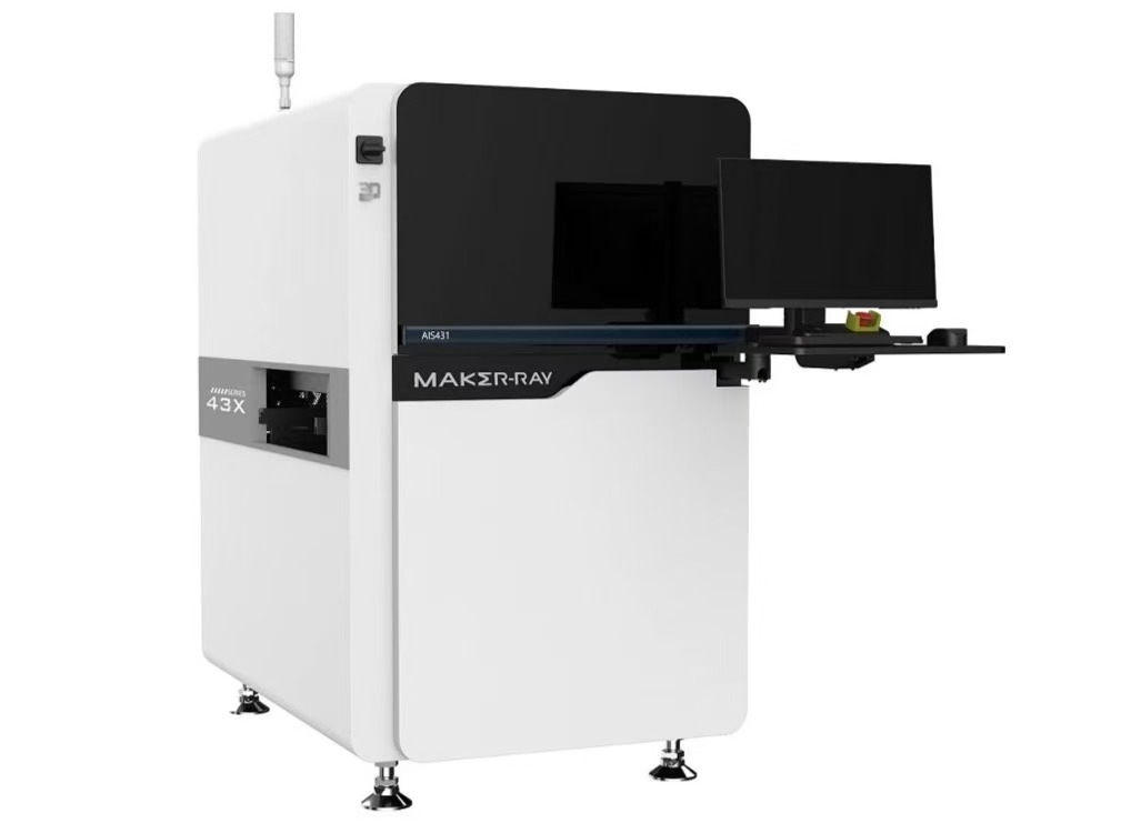
Maker-Ray's new second-generation 3D AOI-AIS431 features significant updates, including enhancements in its design, software, light source, and overall framework. The side-mounted multi-camera panoramic 3D imaging technology, powered by AI deep learning algorithms, provides enhanced accuracy and stability in three-dimensional visualization, making it ideal for high-precision inspection applications. This system employs cutting-edge interactive software and minimalist AI programming to facilitate multi-angle projection and the integration of multi-frequency striped structured light, effectively mitigating the problem of imaging overexposure. Additionally, it features an AI-driven intelligent denoising capability that substantially improves the quality of 3D images of the examined object, providing accurate three-dimensional numbers. This significantly enhances programming speed and genuinely enables enterprises to boost productivity and overall efficiency.
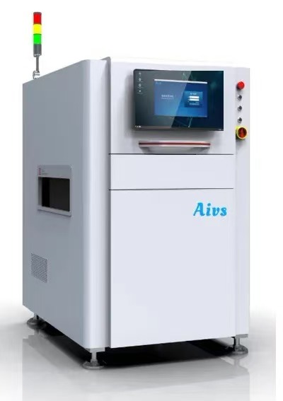
Aivs, specializing in innovative AI vision technology, has created the first intelligent AOI and Automated Visual Inspection (AVI) system that eliminates the need for parameter configuration. This system possesses exclusive intellectual property rights for both its software and hardware components, employing intelligent technology to deliver customers a state-of-the-art solution for intelligent vision applications. The process requires no parameter configuration and offers one-click programming, making it user-friendly for anyone with basic computer skills. The equipment features strong inspection capabilities, AI-enhanced intelligent programming, high-precision programmable structural grating, a high-frame-rate camera, and a four-sided projection scheme. The product employs advanced deep learning algorithms, enabling intelligent and rapid programming. It is user-friendly, with a high detection rate and minimal false alarms.
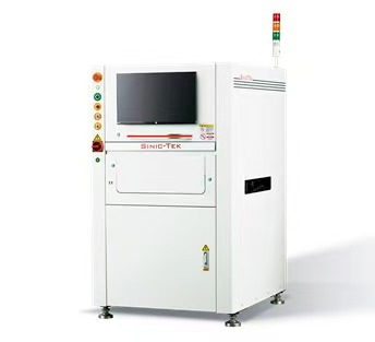
Sinic-Tek, a company deeply engaged in the development of machine vision inspection devices, has introduced the A-510 in-line three-dimensional automated optical inspection system. This cutting-edge equipment features advanced AI-driven seamless puzzle technology, delivering an optical quality that is indistinguishable to the naked eye. It effectively tackles challenges such as image irregularity, unevenness, color inconsistency, and distortion that commonly occur at the junctions between fields of view (FOV) in traditional AOI systems. Consequently, the positioning accuracy of the inspection frame is improved, and the time required for program debugging is reduced. The A-510 incorporates an intelligent program editing method and a parameter configuration system designed like a template, ensuring quick program development and efficient debugging.
AOI can be classified into two types based on their operational methods: online AOI and offline AOI. Online AOI involves the real-time inspection of circuit boards on the SMT production line as they move through AOI equipment. This process allows for the prompt identification and resolution of issues. In contrast, offline AOI involves inspecting circuit boards that have already been removed from the production line. This process facilitates the identification of issues and enables subsequent repairs.
X-ray technology optimizes high-precision welding: from defect detection to cost-effective quality control
In contrast to AOI, X-RAY inspection provides a distinct advantage: It enables non-destructive inspection. X-ray technology can penetrate materials and offer a clear view of a PCB's internal structure, enabling the detection of concealed solder joints in Ball Grid Arrays (BGAs) and Chip Scale Packages (CSPs). These joints are often challenging to access with AOI. The ability to conduct thorough product inspections not only improves production quality but also effectively reduces potential issues by enabling the early detection and correction of welding defects such as false soldering, misaligned solder balls, and bridging. This enhances both the long-term reliability and performance of products. X-ray inspection also proves highly effective in controlling costs. Through early detection of potential issues in the manufacturing process, manufacturers can avoid the rising costs linked to mass-producing defective products, thus eliminating expenses associated with rework and raw material waste.
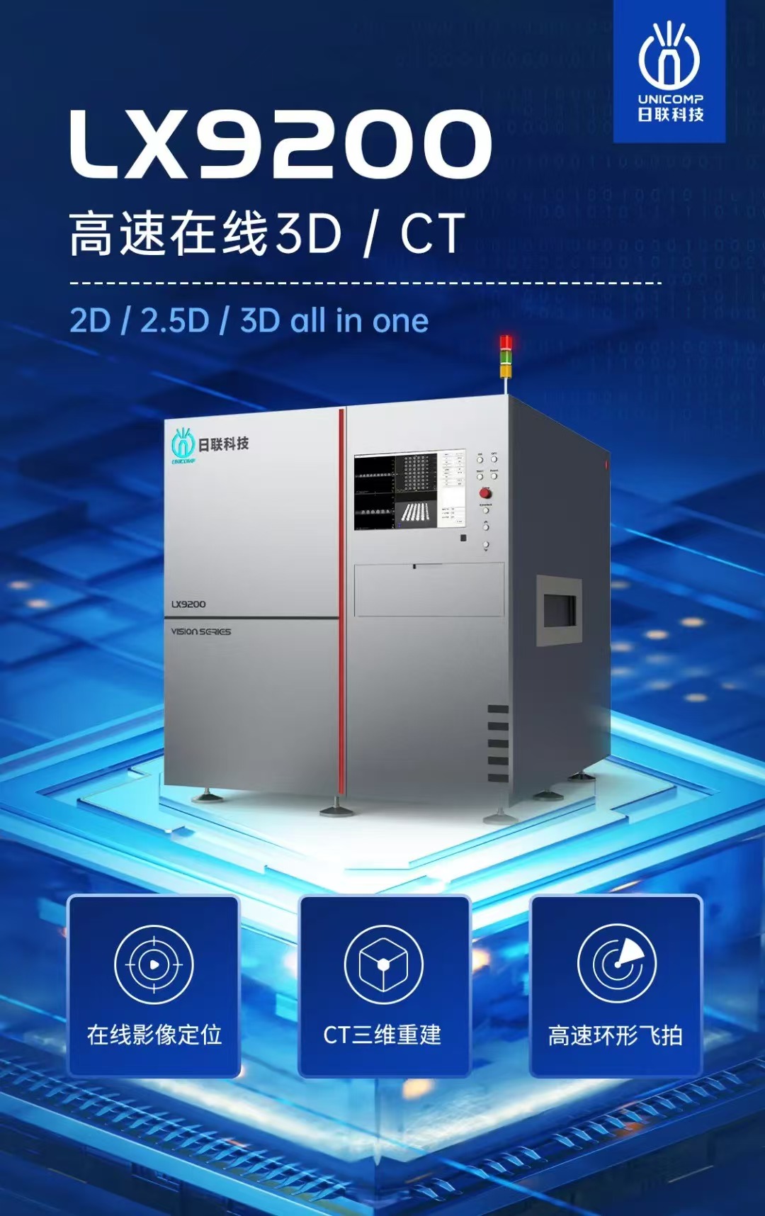
To satisfy the stringent quality inspection standards of automated mass production manufacturers, Unicomp has developed the LX9200, an online 3D micro-focus X-ray automated inspection system. It is primarily used in PCBA processes, including SMT and DIP, and also in BGA, IC, CHIP, PTH, and IGBT applications. It also supports various specialized industries in inspecting defects, including bubbles, bridging, offsets, open circuits, solder quantity, pin presence or absence, and foreign contaminants. The device employs advanced flying trigger image capture technology to facilitate quicker and more stable imaging. The LX9200 incorporates a 360-degree oblique projection technique, along with fast resolution techniques and high-precision iterative 3D reconstruction capabilities. This allows for the efficient and rapid creation of high-quality, high-resolution 3D models of intricate products. The system automatically conducts layered inspections of objects using the reconstructed 3D data. The LX9200 effectively addresses issues such as device interference and ghost image stacking, which are prevalent in 2D inspections. This is particularly beneficial for complex items that have high density, intricate integration, and unique shapes, thereby meeting the varied inspection needs of users.
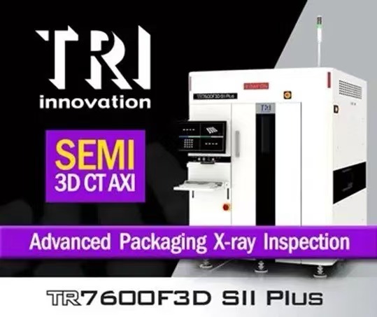
The TR7600F3D SII Plus, launched by TRI Innovation, features a next-generation 110kV X-ray light source and offers high-resolution capabilities with options ranging from 3 to 25 µm. It leverages AI inspection algorithms to significantly enhance defect detection accuracy. The SEMI 3D CT AXI equipment offers thorough inspection of multiple components, such as BGA, QFN, SiP, PTH, PoP, Wire, and Die bond, setting a new industry standard for comprehensive analysis. The 3D AXI TR7600F3D SII Plus is designed specifically for high-reliability electronics manufacturing industries, including advanced packaging, automotive, aerospace, and medical sectors, among others. In the advanced packaging sector, the SEMI 3D CT AXI offers accurate inspection of interconnects in integrated circuit packages, including Micro and C4 bumps. The system utilizes EtherCAT for seamless communication and enhanced connectivity, and incorporates intelligent panel bending control functions to ensure precise alignment between panels. The TR7600F3D SII Plus seamlessly integrates with smart factory lines and selected Manufacturing Execution Systems (MES), ensuring compatibility and reliability for future production processes.
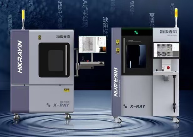
Hikrayin is one of the eight innovative enterprises under Hangzhou-based Hikvision Digital Technology Co., Ltd. It focuses on the application of X-ray imaging technology and is committed to the research, development, manufacturing, and sale of X-ray imaging equipment and intelligent recognition systems for X-ray images. Hikrayin's newly launched intelligent off-line AXI equipment is a versatile, high-precision, non-destructive inspection tool. It features self-developed AI inspection algorithms and a proprietary off-line AXI inspection solution, designed to accommodate two inspection scenarios: offline sampling inspection and comprehensive inspection. This equipment greatly improves inspection speed in small-batch and multi-batch scenarios, while significantly reducing the false positive rate typically linked to manual inspections. Advanced AI algorithms enable single-click detection of welding voids in electronic components such as BGA packages, MOSFETs, and IGBTs. The system features robust interference immunity and automated parameter optimization, delivering rapid quantitative analysis of void percentages while accommodating customized inspection criteria. Hikrayin is dedicated to becoming the leading provider of AXI inspection equipment in the global X-ray inspection market.
Seamark ZM, a veteran in the industry, has developed the AXI9000, a fully automated high-speed CT X-ray inspection system. This equipment features proprietary intelligent inspection software and utilizes a unique 3D/CT reconstruction technology, allowing it to conduct a field of view (FOV) inspection in under 2 seconds, significantly enhancing inspection efficiency. The three-layer gantry system, powered by a linear motor and featuring a high-precision grating ruler, uses an advanced H-height positioning algorithm to achieve precise positioning. The equipment delivers a maximum inspection resolution of 6μm. In high-speed CT scanning, both the number and resolution of projections can be easily adjusted to meet specific requirements, providing versatility for various inspection scenarios. The equipment is equipped with a range of proprietary intelligent inspection algorithms that enable accurate identification and analysis of potential defects, including insufficient solder, bubbles, and the filling rates of DIP components. This technology ensures product quality and improves the overall reliability of the production line.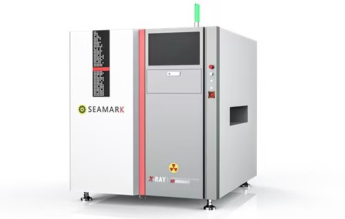
This inspection equipment developed by CYG is specifically designed for products that require wide-angle active alignment processing. It integrates several critical processes, including incoming material inspection, PLASMA cleaning, dispensing, automated optical inspection of dispensing effectiveness, automated focusing, and UV curing. The system supports both fully automated and manual loading and unloading, allowing each process to operate in parallel without interference. The device features a modular design that includes a Pre-AA module, transfer module, and AA module, allowing for quick and easy switching and upgrades to meet varying product requirements. It is engineered to accommodate large wide-angle lenses with a field of view between 45° and 230°. It functions in dust-free environments that uphold a cleanliness level of 100, ensuring high accuracy and efficiency. It also includes features such as dust spot and defect inspection, plasma cleaning, precise dispensing, and UV curing, all aimed at enhancing product quality and production efficiency. The efficient and adaptable design of this AA test device makes it perfect for manufacturing wide-angle camera modules.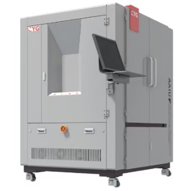
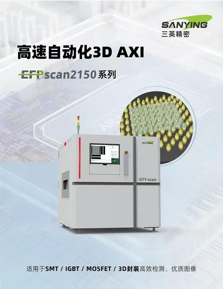
Sanying Precision, an established brand in domestic X-ray three-dimensional CT technology, is meeting the pressing demands of the intelligent electronic manufacturing industry with efficient and accurate automated batch inspection solutions. The company has independently developed an innovative product, the high-speed automated 3D AXI in-line X-ray inspection equipment, to fulfill these requirements. This equipment is designed specifically for the electronics manufacturing industry, including SMT and semiconductors. It employs 3D computed tomography (CT) imaging technology to facilitate high-speed, fully automated in-line inspection of hidden solder joints and layers. It incorporates a state-of-the-art in-line inspection system that utilizes high-speed circular flying trigger scanning technology, along with AI-driven automated identification and analysis. This system integrates seamlessly with the production line to perform 100% rapid inspections and automated product analysis. Automated defect identification and analysis, along with multi-layer dissection, facilitates a thorough and precise evaluation of defective products. It also effectively combines traditional algorithms with AI deep learning techniques to visually depict defect morphology, especially for quality control of hidden solder joints in BGAs and plug-ins.
Diverse inspection methods synergize to establish a new framework for intelligent quality inspection
Inspection methods to ensure product quality and reliability extend well beyond AOI and X-ray techniques. To meet the demand for producing increasingly complex electronic products, the industry has developed a variety of efficient and diverse inspection methods. These inspection methods cover the entire process, from assessing raw materials to evaluating the final product. Each method has specific application scenarios, advantages, and characteristics. They work together to create a comprehensive and multi-dimensional quality monitoring system.
SPEA's 4080 double-sided flying probe tester is regarded as a benchmark in the industry. A single tester can inspect more than 800,000 circuit boards annually. It features a state-of-the-art linear motor on the XYZ axis, achieving speeds of up to 180 needles per second. The addition of a nano-level resolution linear optical encoder enhances testing accuracy, and its natural granite construction significantly minimizes operational vibrations. SPEA's innovative technologies ensure that the 4080 flying probe test equipment remains a leader in the industry, offering unmatched speed, stability, and test accuracy. SPEA's flying probe products offer a wide range of functionalities, including on-off testing, short-circuit testing, power-on testing, burn-in testing, optical testing, and functional testing. They are well-suited for various testing scenarios such as New Product Introduction (NPI), trial production, and maintenance. These products are extensively utilized across multiple industries, including consumer electronics, automotive electronics, medical electronics, military electronics, servers, and aerospace.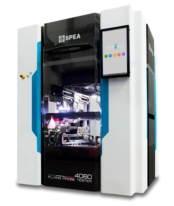
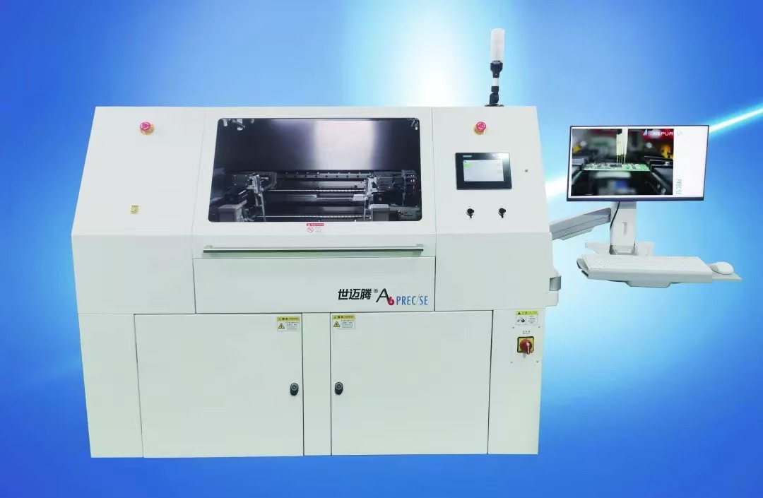
Smarteam has specialized in flying probe inspection for 30 years. The Flying Probe® A6 is a six-pin, multifunctional inspection machine that thoroughly tests printed circuit board assemblies (PCBAs). It is employed for standard in-circuit testing (ICT), new product introduction, maintenance inspections, research and development test automation, and customized design and manufacturing. Flying probes significantly enhance test coverage without requiring fixtures, allowing for testing of fine-pitch, high-density boards and small components. It is suitable for in-line testing of products on SMT production lines. The inspection and fault diagnosis of rework and defective boards enable thorough analysis at the component level. It can also perform powered testing to quickly pinpoint fault locations when utilized with the correct instruments. The system can be equipped with appropriate testing devices and instruments, as well as programmable and swiftly movable probes, to automate manual operations. It performs each task according to a predetermined task list in a fully automated manner. The A6 Flying Probe from Smarteam is a genuine in-line testing tool that includes isolation testing capabilities.
The PILOT VX-PCBA flying probe test system from Seica has enhanced speed and performance. With superior mechanical properties and motion control, it can reduce testing time by up to 50%. Its 12 multifunctional test heads can simultaneously access up to 60 points. Advanced measurement hardware, along with innovative microwave-based measurement technology, significantly improves testing performance. The advanced VIVA software enables various types of parallel tests, further saving time. Additionally, the intelligent analysis function and AI-based algorithms automatically optimize the testing process in real-time while ensuring comprehensive test coverage. The system delivers a robust solution for attaining optimal testing speeds and meeting low to medium volume production requirements. It ensures extensive test coverage and flexibility, making it suitable for prototyping, manufacturing, or repairing any type of circuit board.

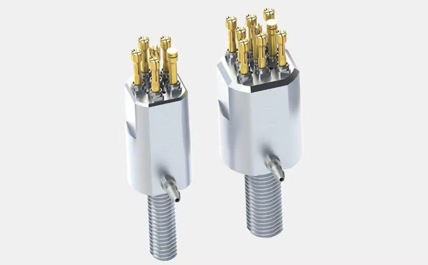
Battery manufacturing encompasses numerous processes and confronts a variety of significant challenges. INGUN's products are used in chemical formulation, cell cycling, end-of-line (EoL) processes, and for measuring open-circuit voltage (OCV), state of charge (SOC), and alternating current/direct current internal resistance (AC/DC-IR). In high-power batteries, the current can reach up to 800 amperes. INGUN provides an array of optimal solutions designed to ensure stable, lossless penetration at the levels of cells, modules, and battery packs. However, it is crucial to ensure that the test solution is both scalable and modular. As a result, the test solution can be designed to accommodate probes of various shapes and technical specifications and to allow for seamless replacement of probes while in operation.
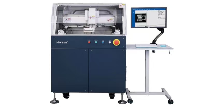
Hiwave specializes in ultrasonic scanning microscopy, a non-destructive imaging technology that uses ultrasonic waves as the medium for propagation. This technique is primarily employed to detect internal defects in semiconductor devices and materials, such as pores, cracks, inclusions, and delamination. The images produced offer a clear and intuitive representation of the test results. This process maintains the integrity of the sample without causing any damage, making it highly applicable in industries such as new energy, semiconductors, and power electronics. The Hiwave S300 ultrasonic scanning microscope, introduced by Hiwave Smart Center, is engineered for defect inspection in water-cooled radiators and similar products. High-frequency ultrasonic technology enables comprehensive inspection of the internal quality and welding processes of water-cooled radiators. In addition, it effectively identifies and visualizes various internal defects, offering an efficient and reliable solution for maintaining product quality control.
Inspection technologies are continually advancing to meet the growing complexity and precision demands of modern electronics manufacturing. The introduction of 3D imaging and AI has significantly enhanced inspection accuracy and efficiency, particularly when addressing tiny components and intricate surface features. The collaborative development and innovation of these technologies are continually advancing SMT inspection technology. productronica Shanghai 2025, scheduled for March 26 to 28, 2025 at the Shanghai New International Expo Centre, will serve as a significant platform for showcasing these new advancements. Leading companies and industry experts from across the globe will convene to showcase their latest research findings and practical applications in SMT inspection technology. Participants will engage in discussions focused on enhancing electronic manufacturing quality and operational efficiency.
Secure premium booths! 2025 booths in high demand!
We extend a heartfelt invitation to electronic manufacturing enterprises both domestically and internationally to participate in the exhibition. Here, you will have an unparalleled opportunity to showcase your latest products and technologies. Leveraging the exhibition's strong influence and wide reach, you can precisely reach target customers and swiftly expand your presence in both domestic and international markets. Moreover, a wide range of exchange activities will foster in-depth collaboration among enterprises. Together, we will explore industry trends, uncover potential business opportunities, achieve mutually beneficial outcomes, and collectively compose a remarkable chapter in the history of the electronics manufacturing industry. There are still a few booths available, so book quickly to seize the competitive advantage in the industry! For further information, please contact Ms. Sinsia at +86 21 20205553.

productronica Shanghai 2027
Click to learn more information about productronica Shanghai 2027.
© Messe Muenchen Shanghai Co., Ltd.
 沪公网安备31011502016746号